Dholera Semiconductor OSAT Hub 2026: Chip Packaging & TP2 Surge

India's sovereign microelectronics revolution achieved a decisive milestone today as equipment installation commenced at the 450-acre Dholera Semiconductor OSAT Hub 2026. Located within Town Planning Scheme 2 (TP2) adjacent to the primary semiconductor fabrication corridor, this world-class Outsourced Semiconductor Assembly and Test (OSAT) and Advanced Packaging facility bridges wafer fabrication and finished chip assembly, fueling unprecedented industrial land appreciation across Dholera Special Investment Region (SIR).
Executive OSAT Briefing: Key Project Benchmarks
Technical specifications approved under the India Semiconductor Mission (ISM) and Gujarat Semiconductor Policy:
- Advanced Packaging Methodologies: 2.5D and 3D System-in-Package (SiP), Flip-Chip BGA, Fan-Out Wafer-Level Packaging (FOWLP), and automated wire-bonding cleanrooms.
- Testing Capacity: High-throughput automated test equipment (ATE) handling over 15 million packaged IC units daily across automotive, telecommunications, and defense chips.
- Cleanroom Class Certification: Class 100 (ISO 5) and Class 1,000 (ISO 6) environments with anti-vibration subterranean foundation slabs and continuous laminar air filtration.
- Direct Fab Integration: Autonomous guided vehicle (AGV) cleanroom tunnels directly transferring completed 300mm silicon wafers from the adjacent Tata-PSMC fab.
Dholera Semiconductor OSAT Hub 2026: Closing India’s Silicon Value Chain
While semiconductor wafer fabrication manufactures microscopic transistors onto silicon discs, the chips cannot function until they are cut, bonded, encapsulated, and rigorously tested under high electrical stress. Dholera Semiconductor OSAT Hub 2026 eliminates India’s historical dependency on overseas packaging houses in Southeast Asia, ensuring that complete microchips are designed, fabricated, packaged, and tested entirely within Gujarat.
The facility features vibration-dampened structural pilings reaching 28 meters below ground, guaranteeing zero mechanical disturbance from adjacent heavy boulevards. Specialized bulk gas pipelines supply high-purity nitrogen, helium, and silane directly through Dholera's subterranean common utility ducts, ensuring continuous cleanroom operation with 99.999% chemical purity.
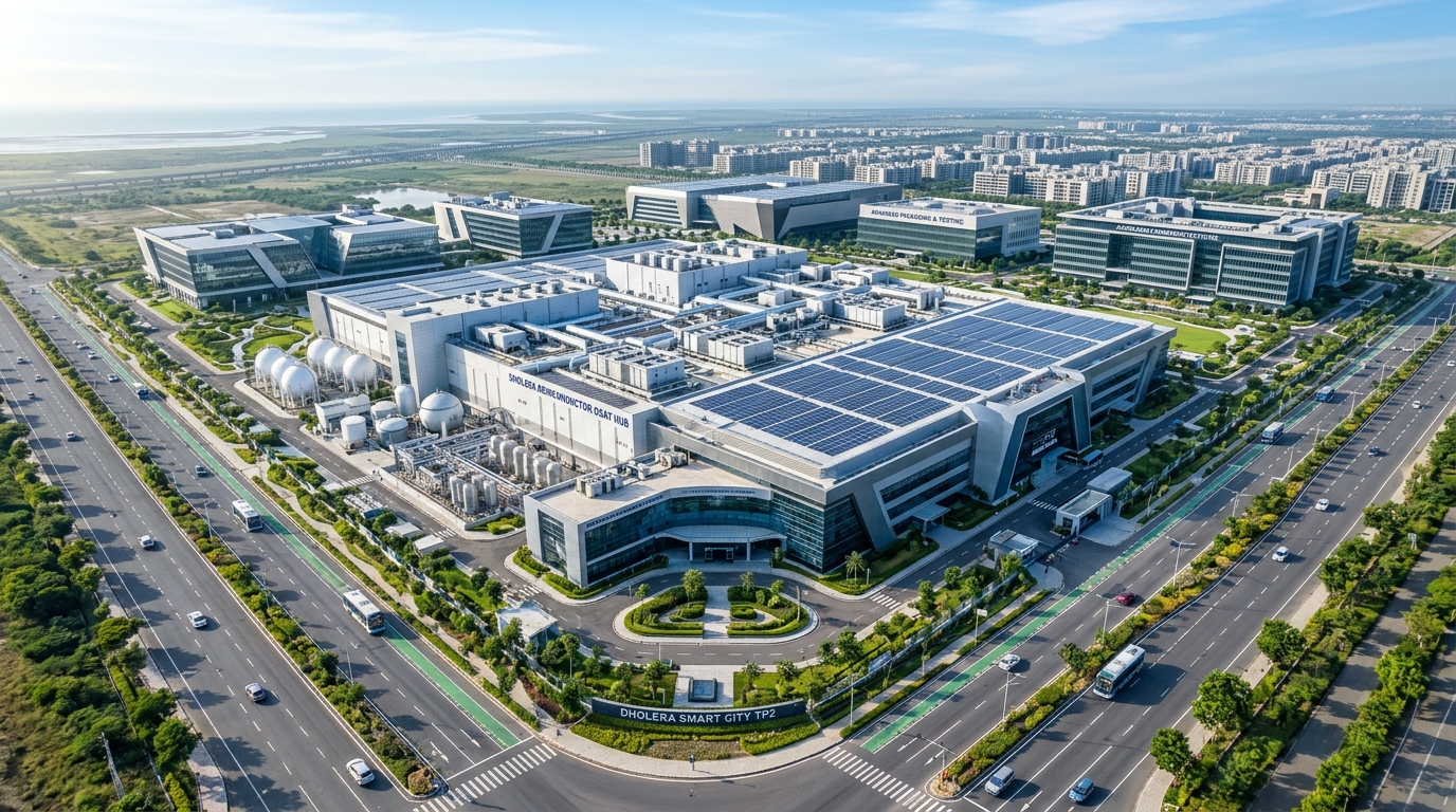
Figure 1: High-altitude aerial view of Dholera Semiconductor OSAT Hub 2026 campus, cleanroom filtration systems, bulk gas spheres, and landscaped arterial boulevards.
Accelerating Vendor Ecosystems & Precision Materials Suppliers
The presence of Dholera Semiconductor OSAT Hub 2026 has triggered an aggressive influx of specialized materials manufacturers into Town Planning Scheme 2. Advanced packaging requires continuous supplies of epoxy mold compounds (EMC), high-purity copper bonding wire, solder spheres, leadframes, and thermal dissipation heatsinks.
Global materials leaders and domestic ancillary ventures are securing contiguous industrial plots within the TP2 vendor park. By operating within the same special economic zone, suppliers deliver raw substrate materials with zero transport customs delay, creating a self-sustaining silicon cluster that reduces final module manufacturing costs by up to 22%.
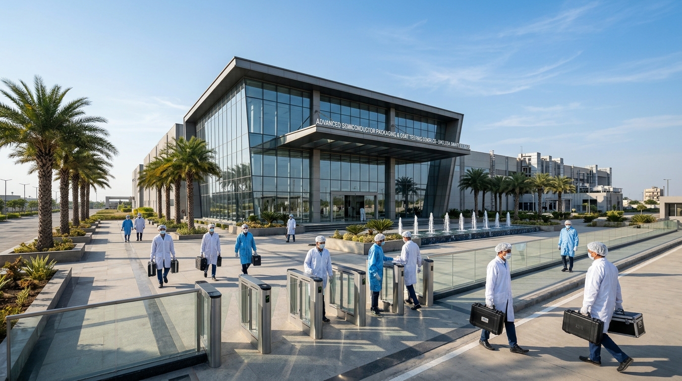
Figure 2: Ground-level architectural perspective of the modern OSAT administrative concourse, biometric cleanroom turnstiles, and semiconductor test engineers.
Multi-Modal Logistics Integration for Global Microchip Exports
The microelectronics export ecosystem of Dholera Semiconductor OSAT Hub 2026 relies on rapid multi-modal transport synchronization:
- Dholera International Cargo Airport: Located 15 minutes away, climate-controlled air cargo facilities enable high-value microchips to board dedicated international freight flights to global electronics hubs.
- Ahmedabad-Dholera Expressway (NH-751): Direct high-speed highway connection links OSAT facilities to assembly lines in Pune, Sanand, and Noida in record time.
- Western Dedicated Freight Corridor (WDFC): Intermodal rail terminals at Bhimnath transport bulk packaging substrates and equipment directly from maritime ports.
- Clean Solar Power Wheeling: 100% green energy delivered from the adjacent 4,400 MW Dholera Solar Park ensures global ESG compliance for carbon-neutral chip exports.
With round-the-clock on-site electronic data interchange (EDI) customs appraisal, packaged semiconductors clear export compliance in under 2 hours, positioning Dholera as an essential hub in the global technology supply chain alongside Taiwan, South Korea, and Japan.
Impact on Real Estate Valuations in TP2 Semiconductor Corridors
The physical activation of advanced packaging infrastructure has driven intense acquisition demand for industrial and commercial plots across Town Planning Scheme 2. Ancillary supply chain vendors, logistics contractors, and executive housing developers are acquiring land surrounding Dholera Semiconductor OSAT Hub 2026, catalyzing strong capital appreciation across verified, title-cleared parcels.
| Corridor / Micro-Market | Zoning Designation & FSI | 2024 Base Rate | Q4 2026 Current Rate | Projected 2028 Value |
|---|---|---|---|---|
| TP2 OSAT & Packaging Tech Spine | High-Tech Semiconductor Ancillary (FSI 3.0) | ₹3,800 – ₹5,200 / sq.yd | ₹9,900 – ₹14,800 / sq.yd | ₹25,000 – ₹34,000 / sq.yd |
| TP2 High-Purity Gas & Vendor Park | Clean Manufacturing & Chemical Supply | ₹3,200 – ₹4,400 / sq.yd | ₹8,000 – ₹12,200 / sq.yd | ₹20,000 – ₹27,000 / sq.yd |
| TP1 Tech Executive Residential Belt | Gated Engineer Townships & Apartments | ₹3,400 – ₹4,600 / sq.yd | ₹8,700 – ₹13,200 / sq.yd | ₹22,000 – ₹29,500 / sq.yd |
Compare TP1 vs TP2 Plug-and-Play Plot Rates
Request the verified 2026 per-sq-yard valuation index, duct connectivity verification, and approved NA/NOC inventory delivered directly to you.
Strategic Advice for Industrial & Semiconductor Land Acquirers
For institutional developers and family offices seeking exposure to Dholera Semiconductor OSAT Hub 2026, acquiring parcels within Town Planning Scheme 2 featuring verified Non-Agricultural (NA) industrial clearance is vital. Parcels situated along arterial utility boulevards offer immediate construction feasibility and superior capital appreciation potential.
Explore Verified High-Growth Opportunities in Dholera SIR
For official national semiconductor mission guidelines, visit the India Semiconductor Mission (ISM) Official Portal or inspect statutory town planning regulations directly with the Dholera Industrial City Development Limited (DICDL) Authority.
Frequently Asked Questions (FAQs)
What is the primary function of Dholera Semiconductor OSAT Hub 2026?
The OSAT hub performs advanced chip assembly, packaging, and high-throughput electrical testing on silicon wafers produced by front-end semiconductor fabs, converting raw wafers into commercial packaged microchips.
How does the OSAT hub coordinate with the Tata semiconductor fab?
Located less than 3 kilometers away in TP2, processed 300mm silicon wafers transfer directly from the fab to the OSAT cleanrooms via autonomous transport vehicles, eliminating overseas shipping delays.
What advanced packaging technologies are being deployed?
The facility utilizes 2.5D/3D System-in-Package (SiP), Flip-Chip Ball Grid Arrays, Fan-Out Wafer-Level Packaging (FOWLP), and automated test equipment handling millions of units daily.
How does the semiconductor hub influence industrial land rates in TP2?
Massive ecosystem supplier investments and tens of thousands of high-tech jobs create intense demand for ancillary industrial plots, logistics warehouses, and residential townships across TP2.
Can investors acquire clear-title plots near the OSAT complex?
Yes, government-approved NA industrial and mixed-use plots with clear legal documentation, verified TP demarcation, and pre-laid utility connections are available across TP1 and TP2.
Download High-Res TP Maps & Free Investor Tools
Planning an investment or tracking infrastructure in Dholera SIR? Access our verified GIS master plans, official mobile app, and free advisory.
Dholera TP 1 – TP 6 Maps
High-definition Town Planning master plans, road grid hierarchy, and zoning boundaries for all sectors.
Dholera Android APK
Real-time plot status, interactive GIS layers, push notifications for breaking news, and offline documents.
1-on-1 WhatsApp Advisory
Direct guidance from Naresh Gohel on NA/NOC clear titles, registry verification, and free site visit cab from Ahmedabad.