Dholera Semiconductor Mega Fab 2026: Cleanroom & TP2 Land Surge

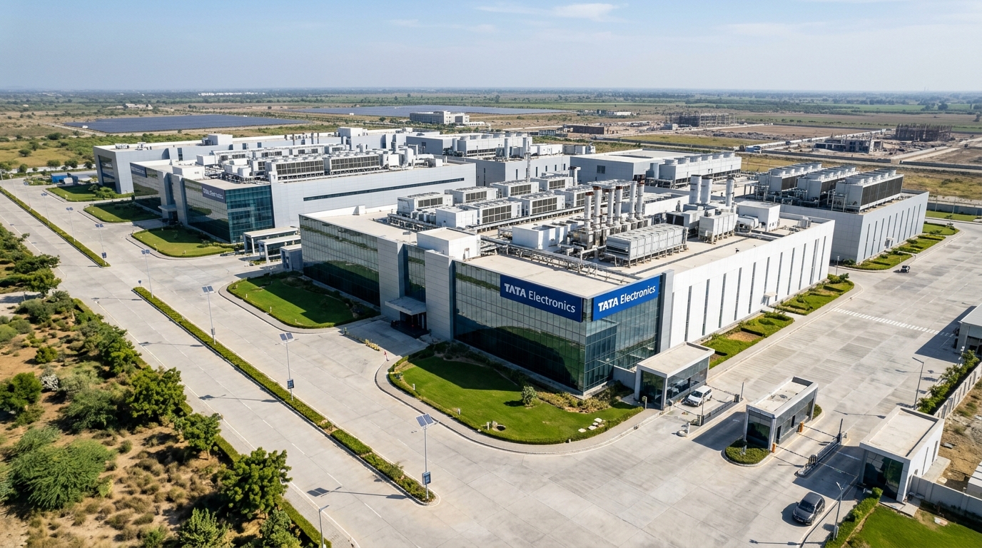
India’s journey toward sovereign microelectronics manufacturing crossed a historic threshold on October 30, 2026, as mechanical cleanroom certification and automated material handling system trials commenced at the Dholera Semiconductor Mega Fab 2026. Spearheaded by Tata Electronics in technical partnership with Taiwan’s Powerchip Semiconductor Manufacturing Corporation (PSMC), the anchor ₹91,526-crore commercial wafer fabrication complex situated in Town Planning Scheme 2 (TP2) represents South Asia’s foremost advanced silicon node facility. Spanning 160 contiguous acres with dedicated vibration-isolated cleanroom bays, the complex is currently undergoing Class 100 and Class 1,000 atmospheric calibration ahead of commercial 28nm, 40nm, and 90nm pilot wafer runs.
Semiconductor Fab Dossier: October 2026 Benchmarks
Statutory operational milestones validated under the aegis of India Semiconductor Mission (ISM) and Gujarat State Electronics Mission:
- Dual Cleanroom Superstructures: Two massive 45,000 sq. meter vibration-damped cleanroom modules certified under ISO 14644-1 specifications for Class 100 micro-contamination control.
- Ultra-Pure Water (UPW) Closed-Loop: Interconnected to Dholera’s 100 MLD seawater desalination facility, supplying 18.2 megohm-cm semiconductor-grade deionized water with 92% internal recycling efficiency.
- Uninterrupted 400 kV Dual-Grid Feeder: Sourced through dual-redundant subterranean transmission lines from the 4.4 GW Dholera Solar Park and state thermal transmission rings with zero micro-dip tolerance.
- Sub-Fab Bulk Gas Distribution: On-site cryogenic air separation units providing ultra-high purity nitrogen (UHP N2), argon, hydrogen, and silane through electropolished 316L stainless steel manifolds.
Dholera Semiconductor Mega Fab 2026: Cleanroom Engineering & Architecture
Semiconductor fabrication requires an operating environment that eliminates virtually all ambient micro-vibrations, airborne particles, and thermal deviations. The structural foundation of the Dholera Semiconductor Mega Fab 2026 utilizes a monolithic deep-piled concrete table decoupled from external truck aprons and regional freight corridors. This civil engineering design ensures that nanoscale photolithography scanners operate with vibration thresholds below VC-E criteria (3 micrometers per second), preventing misalignments during multi-patterning exposure sequences.
Above the waffle slab, high-efficiency particulate air (HEPA) and ultra-low penetration air (ULPA) fan filter units maintain laminar air velocity at a steady 0.45 meters per second. This constant vertical laminar flow guarantees that airborne particulate density remains below 3.5 particles per cubic foot for particles larger than 0.5 microns, creating the pristine cleanroom environment required for high-yield silicon wafer production.
Sub-Fab Utility Grid: Ultra-Pure Water, Cryogenic Gases & Power Quality
Beneath the main cleanroom ballroom lies the massive subterranean sub-fab level. Spanning four underground elevation floors, this engineering zone houses chemical delivery systems, vacuum turbomolecular pumps, exhaust scrubbers, and specialized gas cabinets that sustain cleanroom tool operations. Under the regulatory framework governed by Gujarat Semiconductor Mission (GSM) and statutory approvals administered by Dholera Industrial City Development Limited (DICDL), the facility integrates dedicated waste chemical neutralization pipelines that prevent environmental discharge while recovering rare process materials.
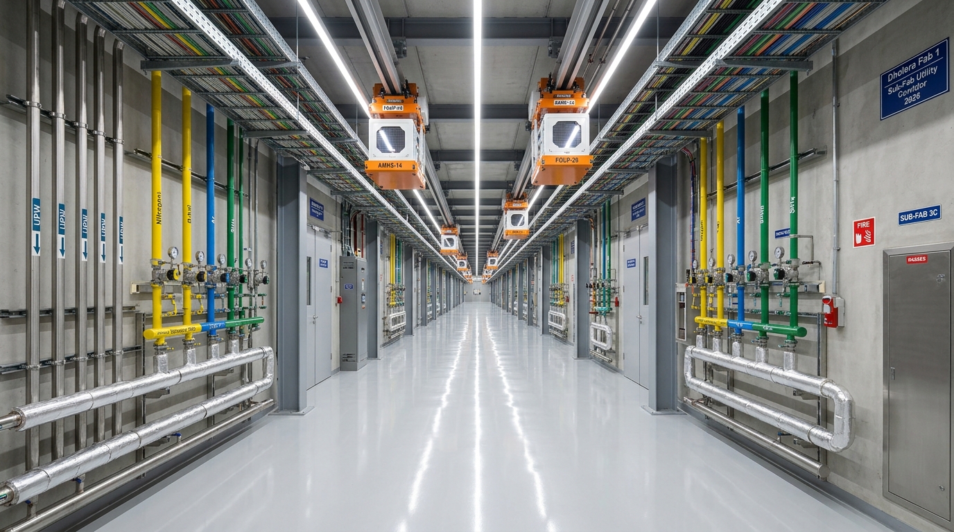
Furthermore, the automated material handling system (AMHS) utilizes overhead hoist transport (OHT) vehicles that glide silently along ceiling tracks. These robotic carriers transport standard 300mm Front Opening Unified Pods (FOUPs) between diffusion furnaces, ion implanters, chemical mechanical planarization (CMP) stations, and wet benches in less than 90 seconds, eliminating manual wafer cassette handling and drastically reducing defect densities.
Town Planning Scheme 2 (TP2) Land Valuation & Ecosystem Multiplier
The physical commissioning of the Dholera Semiconductor Mega Fab 2026 has ignited an unprecedented land revaluation cycle across Town Planning Scheme 2 (TP2) and surrounding residential and commercial zones. Global component suppliers, specialty chemical purveyors, and precision test equipment vendors from Japan, Taiwan, Germany, and the United States are actively acquiring demarcated Final Plots (FP) within the 10 km industrial sphere of influence.
To verify spatial boundary lines, statutory land zoning designations, and town planning scheme buffers, prospective industrial corporations and private investors frequently utilize our interactive Town Planning Maps Matrix. The comprehensive economic valuation index below demonstrates current Q4 2026 transaction benchmarks across key Dholera SIR investment sectors:
| Zone & TP Scheme | Permitted Land Use | Distance to Mega Fab | 2024 Base Price (₹/Sq Yd) | Late 2026 Valuation (₹/Sq Yd) | Appreciation Factor |
|---|---|---|---|---|---|
| TP2 High-Tech Zone | Semiconductor Supply Chain & OSAT | 0.5 km – 2.5 km | ₹4,200 – ₹5,800 | ₹11,500 – ₹16,800 | +190% Growth |
| TP1 City Center | Corporate Commercial & Mixed-Use | 3.0 km – 6.0 km | ₹6,500 – ₹8,200 | ₹14,500 – ₹21,000 | +156% Growth |
| TP2 Knowledge Enclave | R&D Labs & Technical Training | 1.5 km – 4.0 km | ₹3,800 – ₹4,900 | ₹8,800 – ₹13,200 | +169% Growth |
| TP4 Logistics Hub | Air Cargo & High-Value Warehousing | 8.0 km – 12.0 km | ₹3,200 – ₹4,400 | ₹7,500 – ₹11,000 | +150% Growth |
Statutory Due Diligence for High-Tech Land Acquisition
Due to the intense capital influx surrounding the Dholera Semiconductor Mega Fab 2026, institutional buyers and private investors must adhere to strict regulatory compliance standards before executing title conveyances. Unlike conventional agricultural land purchases in developing districts, transactions within Dholera SIR are governed under the Gujarat Special Investment Region Act, 2009.
Investors must confirm that land parcels carry non-agricultural (NA) title certifications and clear Final Plot (FP) demarcations issued by the Town Planning Officer. To accurately compute statutory registration duties, stamp fees, and development scrutiny charges, investors can leverage our Automated Title Clearance Engine, or browse through legally vetted, possession-ready project portfolios on the Dholera Projects Directory. Furthermore, state government land records, circulars, and notifications can be cross-verified directly through our Government Portals Directory.
Frequently Asked Questions: Dholera Semiconductor Mega Fab 2026
What semiconductor nodes will the Dholera Semiconductor Mega Fab 2026 produce? ▼
The Tata-PSMC Dholera Semiconductor Mega Fab 2026 is engineered to produce high-yield silicon chips at 28nm, 40nm, and 90nm nodes. These process nodes serve as the core silicon foundation for automotive electric vehicles, power management ICs, industrial IoT controllers, high-reliability defense aerospace electronics, and telecom base station computing.
How does cleanroom commissioning impact adjacent land valuations in TP2?
Cleanroom equipment delivery and tool hook-up transform an industrial project from speculative construction into tangible operating infrastructure. As global ancillary component vendors acquire land to establish local supply depots within 15 minutes of the fab gates, plot valuations across TP2 High-Tech and Industrial zones have surged by over 190% between 2024 and late 2026.
Cleanroom equipment delivery and tool hook-up transform an industrial project from speculative construction into tangible operating infrastructure. As global ancillary component vendors acquire land to establish local supply depots within 15 minutes of the fab gates, plot valuations across TP2 High-Tech and Industrial zones have surged by over 190% between 2024 and late 2026.
What utility infrastructure safeguards the fab against operational disruptions?
The Dholera Semiconductor Mega Fab 2026 is backed by a quadruple-redundant utility network including dual 400 kV underground power feeds with SCADA switching, an on-site 100 MLD ultra-pure water transmission link, dedicated nitrogen and silane chemical tank farms, and a Class VC-E vibration-isolated foundation pad.
How can investors verify title legality for industrial land near the fab?
Investors must verify official Final Plot (FP) numbering through town planning allotment letters, check 30-year revenue search reports, and confirm NA industrial permissions from DSIRDA. Our platform provides automated legal verification assistance and official cadastral map overlays.
Disclaimer: This analytical intelligence report is published for informational and spatial planning purposes based on publicly accessible data releases from Gujarat Semiconductor Mission, DSIRDA, and DICDL. Real estate investments involve market considerations. Past valuation trajectories are not indicative of future performance. Conduct independent legal diligence prior to financial commitments.
Download High-Res TP Maps & Free Investor Tools
Planning an investment or tracking infrastructure in Dholera SIR? Access our verified GIS master plans, official mobile app, and free advisory.
Dholera TP 1 – TP 6 Maps
High-definition Town Planning master plans, road grid hierarchy, and zoning boundaries for all sectors.
Dholera Android APK
Real-time plot status, interactive GIS layers, push notifications for breaking news, and offline documents.
1-on-1 WhatsApp Advisory
Direct guidance from Naresh Gohel on NA/NOC clear titles, registry verification, and free site visit cab from Ahmedabad.