Dholera Semiconductor Hub: Fujifilm & DHL TP2 Land Surge

As Tata Electronics crosses the 50% civil construction milestone on India's flagship ₹91,526-crore commercial wafer fab, the Dholera Semiconductor Hub has triggered a massive second-wave industrial migration across Town Planning Scheme 2 (TP2). With Japanese chemical titan FUJIFILM Corporation committing ₹800 crore toward specialized electronic chemical plants, global logistics leader DHL breaking ground on cleanroom warehousing, and lithography titan ASML establishing dedicated engineering bases, Dholera Special Investment Region (SIR) is cementing its stature as the undisputed silicon capital of South Asia.
Executive Overview: The Ancillary Influx at Dholera Semiconductor Hub
A semiconductor manufacturing fab cannot function in isolation. Producing microchips at nanometer scale requires a hyper-synchronized web of ultra-pure chemical formulators, cryogenic gas suppliers, precision quartz fabricators, and specialized cold-chain logistics providers within a 15-minute radius of the cleanroom bays.
Under the proactive aegis of the Gujarat Semiconductor Mission (GSM) and Dholera Industrial City Development Limited (DICDL), the state has allocated dedicated acreage in TP2 specifically zoned for international tier-1 semiconductor vendors. This high-density concentration of capital expenditure has unleashed unprecedented institutional demand for industrial, logistics, and executive residential plots across Dholera SIR.
1. Fujifilm’s ₹800-Crore Semiconductor Materials Facility
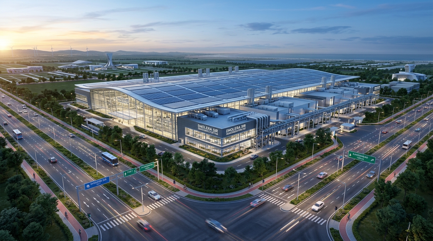
The headline development galvanizing institutional land investors in late 2026 is FUJIFILM Corporation’s strategic partnership with Tata Electronics. Backed by a phased capital deployment exceeding ₹800 crore (~$83 million), Fujifilm is establishing an advanced semiconductor materials fabrication complex in TP2.
This specialized facility will locally produce mission-critical front-end chip manufacturing inputs:
- Electronic Chemical Mechanical Planarization (CMP) Slurries: High-precision abrasive chemical suspensions essential for microscopic wafer polishing.
- Advanced Photoresists & Formulations: Light-sensitive polymer resins used to etch microchip circuitry under ultraviolet lithography scanners.
- Post-CMP High-Purity Cleaners: Proprietary chemical solutions preventing surface ionic contamination on finished silicon wafers.
By anchoring domestic production of specialty chemicals in the Dholera Semiconductor Hub, Fujifilm significantly decreases India’s reliance on East Asian supply chains while creating over 1,800 direct high-salaried engineering positions.
2. DHL Group’s Specialized Semiconductor Logistics Hub
Handling raw 300mm silicon wafers, optical projection masks, and hazardous precursor chemicals requires logistics infrastructure far beyond standard commercial freight. Addressing this imperative, global logistics titan DHL Group has announced a specialized ₹50-crore semiconductor logistics center in Dholera SIR, scheduled for operational commissioning in mid-2027.
Engineered with vibration-isolated foundations and Class-1000 cleanroom sorting zones, this multimodal depot links directly to the newly operational Ahmedabad Dholera Expressway and the upcoming Navagam International Cargo Terminal, providing end-to-end temperature-controlled transit for global chip components.
Compare TP1 vs TP2 Plug-and-Play Plot Rates
Request the verified 2026 per-sq-yard valuation index, duct connectivity verification, and approved NA/NOC inventory delivered directly to you.
3. Town Planning Matrix: Industrial & Residential Valuation Surge
The influx of multinational corporations into the Dholera Semiconductor Hub is driving profound land revaluations across designated Town Planning (TP) boundaries. Investors targeting asymmetric appreciation must align capital with statutory zoning frameworks:
| Town Planning Scheme | Zoning Designation | Anchor Drivers | 2024 Base Price | 2026 Valuation | Growth Catalyst |
|---|---|---|---|---|---|
| TP2 High-Tech Zone | Fab & Ancillary Industrial | Tata Mega Fab, Fujifilm Plant, ASML | ₹5,500 – ₹7,500 / sq yd | ₹14,000 – ₹22,000 / sq yd | Subterranean Gas/Power Redundancy |
| TP1 Residential Core | High-Density Housing & Commercial | Executive Townships, Schooling Hubs | ₹4,500 – ₹6,000 / sq yd | ₹10,500 – ₹16,000 / sq yd | 35,000 High-Income Tech Workforce |
| TP3 Logistics Gateway | Warehousing & Multimodal Freight | DHL Hub, DFC Railway Siding | ₹3,000 – ₹4,200 / sq yd | ₹7,200 – ₹11,000 / sq yd | Dedicated Freight Corridor Link |
4. Land Due Diligence: Navigating TP Schemes Safely
With capital flowing aggressively into plots surrounding the Dholera Semiconductor Hub, private investors must observe disciplined revenue verification protocols to avoid unzoned or non-conforming parcels:
- Verify Final Plot (FP) Status: Ensure the land has received its conclusive Final Plot demarcation under the Gujarat Town Planning and Urban Development Act (GTPUDA). Interactive FP boundaries can be surveyed on our Dholera TP Maps Matrix.
- Audit Revenue Title Clearance: Utilize our institutional Automated Title Clearance Engine to verify 30-year revenue records (7/12 extracts, Form 6 index, and encumbrance certificates) directly from Gandhinagar land registries.
- Focus on RERA-Registered Layouts: Allocate capital exclusively to sanctioned gated communities possessing active Gujarat RERA registration numbers. Explore our curated catalog of verified residential developments.
- Consult Specialized Local Land Advisors: For bespoke portfolio allocations, on-ground demarcation surveys, and corporate registry filings, consult our strategic advisory desk.
5. Strategic Portfolio Allocations for Enterprise & NRI Investors
When structuring a multi-crore land investment strategy around the Dholera Semiconductor Hub, institutional asset managers divide exposure into three distinct investment horizons:
First, Core Industrial Allotments situated directly adjacent to TP2's 70-meter arterial avenues offer the highest rental yield potential, as Tier-2 chemical, packaging, and gas suppliers actively compete for long-term ground leases.
Second, High-Density Residential Townships within TP1 provide unmatched capital safety. With more than 35,000 process engineers, cleanroom operators, and international corporate expatriates requiring premium housing, gated villa communities and multi-story luxury apartments will experience severe supply deficits by late 2027.
Third, Logistics and Cold-Storage Parcels flanking the TP3 transport corridor benefit directly from proximity to DHL's air-conditioned supply depot and the Western Dedicated Freight Corridor (DFC). Review comprehensive project feasibility with our verified advisors today.
Schedule a Private Semiconductor Corridor Land Briefing
Speak with our senior land strategists to review demarcated Final Plots situated within a 3-kilometer radius of the Tata Fab and Fujifilm facility in TP2.
Connect With Land Specialist →Frequently Asked Questions About Dholera Semiconductor Hub
What companies are currently investing in the Dholera Semiconductor Hub?
The core anchor is Tata Electronics with its ₹91,526-crore 300mm wafer fab partnered with Taiwan’s PSMC. Key global ancillaries investing directly include FUJIFILM Corporation (₹800-crore chemical plant), DHL Group (₹50-crore cleanroom logistics depot), and ASML (direct lithography engineering support operations).
How does the semiconductor hub impact land prices in TP1 and TP2?
The demand for high-tech ancillary facilities in TP2 and high-income executive housing in TP1 has catalyzed plot appreciation rates ranging from 120% to 190% between 2024 and 2026. Ready-possession plots with plug-and-play utility tapping command the highest liquidity.
What infrastructure makes Dholera suitable for advanced semiconductor fabs?
Dholera SIR provides dedicated 24/7 subterranean utility ducts, redundant 66kV electrical substations, a 4,400 MW solar microgrid, daily supply of tertiary treated demineralized water, and seamless access via the 109-km Ahmedabad Dholera Expressway and international cargo airport.
Can private individual investors purchase plots near the semiconductor corridor?
Yes. Private Indian citizens and NRI investors can legally purchase clear-title, NA-sanctioned residential and commercial Final Plots (FP) in Town Planning Scheme 1 (TP1) and TP2 through authorized RERA-approved layouts.